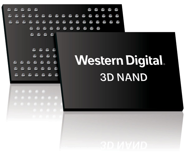
Western Digital Corp. (NASDAQ: WDC) today announced successful development of its second-generation, four-bits-per-cell architecture for 3D NAND. Implemented for the company’s 96-layer BiCS4 device, the QLC technology delivers the industry’s highest 3D NAND storage capacity of 1.33 terabits (Tb) in a single chip. BiCS4 was developed at the joint venture flash manufacturing facility in Yokkaichi, Japan with our partner Toshiba Memory Corporation. It is sampling now and volume shipments are expected to commence this calendar year beginning with consumer products marketed under the SanDisk brand. The company expects to deploy BiCS4 in a wide variety of applications from retail to enterprise SSDs.
“Leveraging Western Digital’s silicon processing, device engineering and system integration capabilities, the QLC technology allows 16 distinct levels to be sensed and utilized for storing data,” said Dr. Siva Sivaram, executive vice president, Silicon Technology and Manufacturing at Western Digital. “BiCS4 QLC is our second generation four-bits-per-cell device, and it builds on the learnings from our QLC implementation in 64-layer BiCS3. With the best intrinsic cost structure of any NAND product, BiCS4 underscores our strengths in developing flash innovations that allow our customers’ data to thrive across retail, mobile, embedded, client and enterprise environments. We expect the four-bits-per-cell technology will find mainstream use in all these applications.”
For more information, log on to www.wdc.com.

