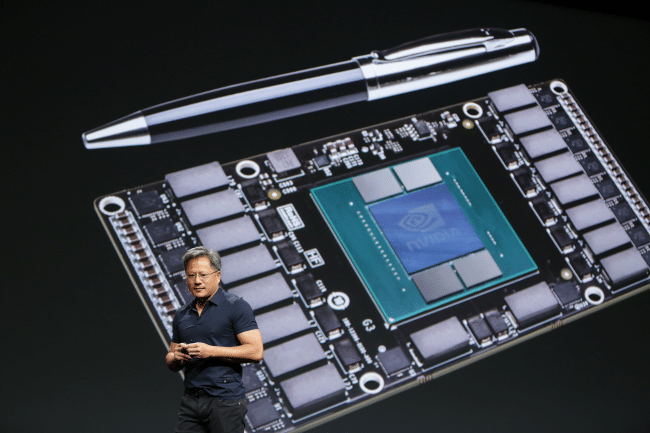
GPU Technology Conference (25th March 2014) – During a keynote speech at our annual GPU Technology Conference in San Jose, Calif., NVIDIA CEO Jen-Hsun Huang updated our public GPU roadmap with the announcement of Pascal, the GPU family that will follow this year’s Maxwell GPUs.
Named for 17th century French mathematician Blaise Pascal, our next-generation family of GPUs will include three key new features: stacked DRAM, unified memory, and NVLink.
- 3D Memory: Stacks DRAM chips into dense modules with wide interfaces, and brings them inside the same package as the GPU. This lets GPUs get data from memory more quickly – boosting throughput and efficiency – allowing us to build more compact GPUs that put more power into smaller devices. The result: several times greater bandwidth, more than twice the memory capacity and quadrupled energy efficiency.
- Unified Memory: This will make building applications that take advantage of what both GPUs and CPUs can do quicker and easier by allowing the CPU to access the GPU’s memory, and the GPU to access the CPU’s memory, so developers don’t have to allocate resources between the two.
- NVLink: Today’s computers are constrained by the speed at which data can move between the CPU and GPU. NVLink puts a fatter pipe between the CPU and GPU, allowing data to flow at more than 80GB per second, compared to the 16GB per second available now.
- Pascal Module: NVIDIA has designed a module to house Pascal GPUs with NVLink. At one-third the size of the standard boards used today, they’ll put the power of GPUs into more compact form factors than ever before.
Pascal is due in 2016.
For more details on Pascal and Stacked Memory see this Parallel Forall post by NVIDIA Senior Director of Architecture Denis Foley.

Ads by Google

